Scintillation Detectors


Scintillator Reference Material
Temperature Influence on Material Response
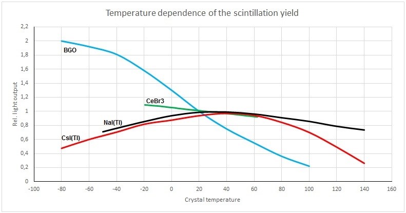
The light output (number of photons per MeV gamma) of most scintillators is a function of temperature. This is caused by the fact that in scintillation crystals, radiative transitions, responsible for the production of scintillation light, compete with nonradiative transitions (no light production). In most scintillation crystals, the light output is quenched (decreased) at higher temperatures. An example of the contrary is the fast component of BaF2 of which the emission intensity is essentially temperature independent.
The scintillation process usually involves production, transport and quenching centres. Competition between these three processes each behaving differently with temperature causes a complex temperature dependence of the scintillation light output. Below the temperature dependence of some common scintillation crystals is shown.
For most applications, the combination of the temperature dependent light output of the scintillator together with the temperature dependent amplification of the light detector should be considered.
The doped scintillators NaI(Tl), CsI(Tl) and CsI(Na) show a distinct maximum in intensity whereas many undoped scintillators such as BGO show an increase in intensity with decreasing temperature. The temperature dependence of the Ce doped scintillators LBC, CeBr3 and YAP:Ce is significantly less than that of other scintillators.
Voltage Dividers & Preamplifiers
Scintillation detectors usually employ a Voltage Divider (VD) network to operate the PMT. This sometimes called “bleeder network” defines a potential (voltage) difference between the cathode, dynodes and anode of the PMT. The exact design of this network is of influence for proper working of the scintillation detector. Some details of voltage divider networks are discussed below. The descriptions below are not exhaustive; for more details we refer to the photomultiplier manufacturer’s literature.
Positive or Negative High Voltage?
It is possible to operate a photomultiplier tube in two ways:
- A. anode at positive potential (cathode at ground)
- B. anode at ground (cathode at negative potential)
For measurements of DC anode current such as in some X-ray applications, option B is the only choice since in the first option the anode must be separated from the follow-up electronics by means of a high voltage capacitor.
On the other hand, option A is used for most standard applications since the m -metal shield should be preferably at cathode potential. Option A implies that cathode, detector mass (ground) and shield are all connected together. In option B, the shield must be very well insulated from the detector mass and special construction requirements apply.
Negative high voltage is required for some fast timing applications where the possibility of discharges between the cathode of the PMT and the m -shield are to be avoided. These PMTs are operated at more than 2 kV for fast response.
Voltage dividers for detectors operated at positive high voltage can be wired with a single connector for signal and HV. At the electronic side, these can be separated using a simple splitter, as illustrated in fig. 8.2
The design of the voltage divider influences the performance of a detector. At high count rates, the voltage across dynodes may drop and the average bleeder current should always be defined as at least 10 times larger than the average anode current in the detector. A standard resistor value between dynodes is 470kW. This is a compromise between bleeder current and gain stability which is sufficient for count rates up to approximately 50.000 c/s.
Voltage dividers may be linear (most common), tapered or specially stabilized with Zener dynodes or transistors.
The number of possibilities is large. A very important aspect is the potential (electric field) between the cathode and the first dynode of the PMT. In any case, this potential should be sufficient to ensure a good photoelectron collection efficiency. Usually, this voltage is prescribed by the PMT manufacturer.
The gain of a scintillation detector varies with each PMT and is also strongly influenced by the exact design of the voltage divider. If the absolute detector gain is of Importance, it can be defined as: the output voltage (in e.g. 1MW ) at a specific operating voltage of the PMT for a certain energy absorbed in the detector.
PMTs can be selected on gain but adjustment of the gain of the detector by varying the voltage in the VD by means of a precision potentiometer is much more convenient. Extra options on voltage dividers are e.g. a gain potentiometer, an extra dynode output or a focus potentiometer.
SCIONIX can design the voltage divider best suited for your application without any additional cost.
Plug-on or Integrated?
Voltage Dividers and other electronics can be incorporated into the scintillation detector. In this case, the resistor network is directly soldered onto the pins of the PMT which implies a minimal length of the assembly. For low background applications this is the preferable option.
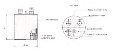
The connector(s) for high voltage and signal are located at the back of the assembly. Also, flying leads are an option. When it is expected that detectors have to be interchanged often it may be preferable to use a so-called “plug-on” option in which case the voltage divider and associated electronics are mounted in a small housing with the same diameter as the detector which is plugged on the pins of the base of the PMT. Most frequently used PMT bases in this respect are the 12 pin JEDEC B12-43 base for 38 mm diameter PMTs and the 14 pin JEDEC B14-38 base for 51, 76 and 127 mm diameter PMTs. These are also the standard bases for scintillation detectors supplied without voltage divider. Below some examples are presented.
Voltage Dividers and Preamplifiers
A PMT signal will be attenuated in a long cable and when signals have to be transported over more than say 10 m of cable this effect cannot be neglected. Signals even may become deformed and signal differences between a set of detectors having different cable lengths can be a problem.
Furthermore, the signal that is to be fed into a main amplifier (also called shaping amplifier or spectroscopic amplifier) needs to have a certain pulse fall time (typically 50 m s) in order to allow proper pole-zero and base-line correction. This effect is especially important at high count rates.
To solve the above problems, scintillation detectors can be supplied with a built-in (or plug-on) voltage divider/ preamplifier. This amplifier has an output impedance of 50 W for proper matching to the most frequently used cable impedance (reflections). Usually, the end stage of this amplifier is based on the principle of an emitter follower.
The standard SCIONIX voltage divider/ preamplifier the VD (12) 14 / E2 is an example of this suited for a wide variety of PMTs. This amplifier operates with a wide variety of voltages, is very fast (rise time < 50 ns) and can drive cable lengths of 100 m or more. Varieties for ultra low power consumption exist. The amplifier is very small so that it will fit in almost every scintillation detector. Please consult JCS for your specific requirements regarding signal shape, power consumption etc.
Connectors
Often, high voltage, signal and preamplifier power are fed in via separate connectors. The SCIONIX standard connector for high voltage is the SHV(Super High Voltage) connector, the most frequently used standard in nuclear electronics. For signals, BNC connectors are the standard and for preamplifier power signals, the dual LEMO type 0 and the 9 pin sub-D connector are normally used.
Other possibilities are e.g. flying leads options, water tight connectors, MHV, TNC, PET-100 and different types of LEMO or FISHER connectors.
Power HV and signal can also be fed in (out) via a single large multipole connector
Built-in High Voltage Generators and Other Electronics
Recent developments in hybrid circuitry have allowed to incorporate a number of other electronic components into the scintillation detector assembly which eliminates in some applications the necessity of NIM based electronics.
An example of the above is the scintillation detector with a built-in High /oltage Generator( – HV option, see section 6). This is a small Cockroft – Walton generator which produces the high voltage required to operate a PMT. This unit only requires a DC voltage of + 5 V or + 12 V and uses only 100 mW of power. The unit is fully integrated with the PMT so there are no high voltage leads anywhere in the assembly. The gain of the PMT is maintained even at high anode currents (up to 100 m A) and the unit adds only 50 mm to the length of the PMT. The high voltage can be factory set, precision potentiometer adjustable or set by a 0 – 1 V regulating voltage. Below the advantages are summarized.
Advantages built-in high voltage generators:
- Compact
- Low power consumption
- Sealed
- High gain stability versus count rate
Besides the above mentioned preamplifiers it is also possible to incorporate e.g. shaping amplifiers (spectroscopic amplifiers) or Single Channel Analyzers (SCAs) into a detector assembly. All these components, constructed as small SMD or hybrid circuits, are very small in dimension. Specific parameters of these devices can be defined by the user since the standard models can be easily adapted. Please consult JCS for more details.
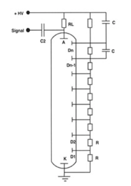
fig. 8.1
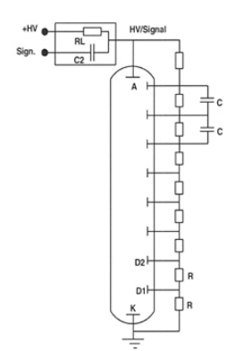
fig. 8.2